Contents — find the section you need
Background and reading guide
Background Units used in specifications, such as voltage, current, distance and time.
Fundamentals · Explanations of principles, structure and trade-offs.
An AI inference accelerator is a chip purpose-built to run the "inference" pass of a trained neural network — the forward computation only — at far higher energy efficiency than a CPU or GPU. The core physical principle is simple: converting weights trained in 32-bit floating point (FP32) into a lower-precision representation such as 8-bit integers (INT8) — quantization — lets the same compute units and the same memory bandwidth push through far more parallel operations. This article does not compare SBCs (single-board computers) as whole systems; instead it focuses squarely on the design philosophy and the quantization principle behind accelerator chips dedicated purely to inference: Google Coral (Edge TPU), Intel Movidius (Myriad X), and NVIDIA Jetson Orin NX.
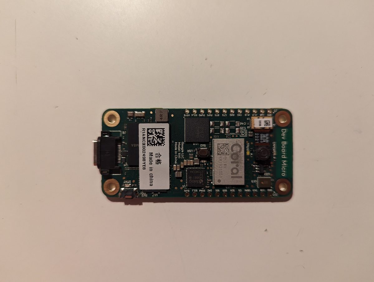 Google Coral Dev Board Micro
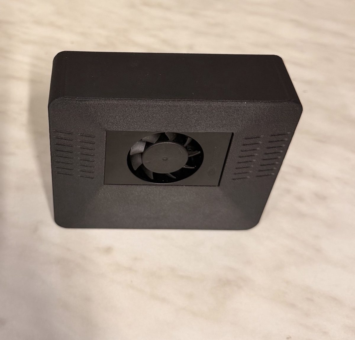 "ClawBox," built on an NVIDIA Jetson Orin Nano (2026, ID Robots)
Images: Hardware PXL 20231201 152957218 (53388218926)(Thomas Amberg, CC BY-SA 2.0) / ClawBox AI assistant device (2026) - front(Kkralev, CC BY-SA 4.0), both via Wikimedia Commons.
.jpg)
_-_front.jpg)
Principle: what INT8 quantization actually does
The most common way to squeeze FP32 weights and activations into 8-bit integers is linear (affine) quantization. The formula converting a real value x into an integer q is:
Here s is the scale (the real-valued width of one integer step), z is the zero-point (the offset telling which integer step corresponds to real zero), and b is the bit width (8 for INT8). At inference time the value is approximately recovered as x \approx s(q-z). What this quantization means in practice is that how tightly the value distribution can be bounded directly determines how much accuracy is lost. With the same 256 steps (INT8), a narrow value range keeps the width of each step — the quantization error — small; a range widened by outliers spreads the same 256 steps thinner, coarsening the representation of the typical values that make up the bulk of the distribution.
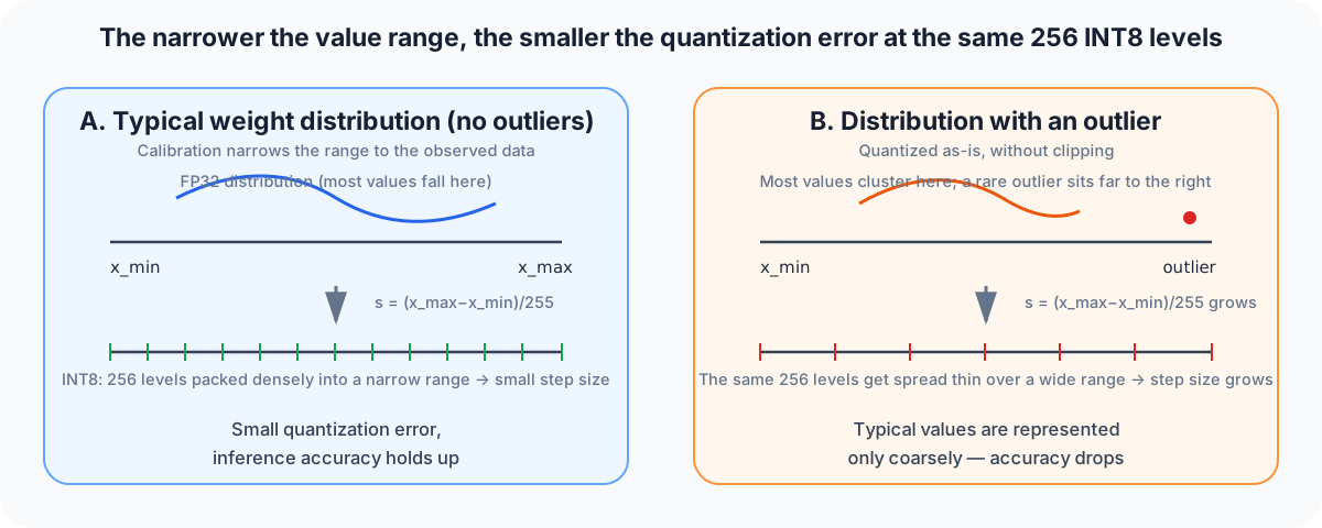
Diagram: Duskcoil. Illustrates how the presence or absence of "calibration" — bounding the value range using real measured data — significantly affects quantization error even at the same bit width.
Deciding this value range is the calibration step, and quantization broadly follows two approaches. Post-Training Quantization (PTQ) simply runs a small amount of representative data through the trained FP32 model and computes the scale s from each layer's observed output range — a lightweight approach, but one prone to larger accuracy loss on models with many outliers. Quantization-Aware Training (QAT) simulates the rounding error introduced by quantization during training itself, updating weights accordingly; this suppresses accuracy degradation at the cost of a retraining pass. The Edge TPU Compiler, TensorRT, and OpenVINO all support both approaches, but since most edge inference chips quote their catalog performance (TOPS) assuming INT8, the practical fork in the road is whether PTQ yields sufficient accuracy or whether it's necessary to switch to QAT.
There's also a further wrinkle: VPUs (Vision Processing Units) designed around 2017, such as the Movidius Myriad X, used FP16 (half-precision floating point) rather than INT8 as their primary compute precision. FP16 halves memory footprint and bandwidth demand relative to FP32 while — because it retains an exponent field — representing a wide dynamic range without needing INT8-style range calibration. It doesn't reach the parallelism INT8 can achieve, though, which is one reason the later Coral Edge TPU and Jetson's Tensor Cores, both built around INT8-first dedicated data paths, post several times the TOPS/W.
Principle: the graph compiler as a second axis of inference speedup
Alongside quantization, what a trained model gets compiled down into for a given chip's instruction set is the other major factor in real-world throughput. A model exported from TensorFlow Lite or ONNX is, on its own, a generic graph executed layer by layer in sequence on a CPU. Each vendor's compiler applies roughly three kinds of optimization to this graph.
- Operator fusion: A sequence like Convolution→BatchNorm→ReLU is merged into a single fused kernel, keeping intermediate results in registers rather than writing them back to memory, cutting the number of memory accesses.
- Layout transformation: The CPU-preferred NCHW (channel-first) layout and the vector-unit-preferred NHWC (channel-last) layout are re-selected to match the actual memory access pattern of the target hardware.
- Compilation to a fixed graph: Some compilers, such as the Coral Edge TPU Compiler, accept only a fully fixed graph built entirely from supported operators, disallowing dynamic shapes or unsupported ops outright. If even a single unsupported operator appears in the model, execution splits between CPU and the Edge TPU around it, and the resulting bidirectional data transfer cost can substantially erode speed.
NVIDIA's TensorRT and Intel's OpenVINO take a more flexible "partial offload" approach — falling back unsupported operators to the CPU while offloading the rest to the accelerator — whereas the Coral Edge TPU Compiler is closer to an all-or-nothing choice between a fully supported graph and no acceleration at all. This distinction doesn't show up in hardware metrics like the TOPS/memory-bandwidth tradeoffs covered in the SBC comparison article — it's a difference in the software stack's design philosophy, and it substantially affects the real cost of porting a model.
Major chip comparison: Coral, Movidius, Jetson
| Product | Precision | AI performance | Power | Interface | Price |
|---|---|---|---|---|---|
| Google Coral Edge TPU (USB Accelerator) | INT8 only | 4 TOPS (2 TOPS/W) | 2W | USB 3.0 | ~$75–99 (2019 launch) |
| Intel Movidius Myriad X (Neural Compute Stick 2) | Mainly FP16 | ~4 TOPS-equivalent (no official published figure) | ~1.5–2.5W | USB 3.0 | ~$79–99 (2018 launch, now discontinued) |
| Hailo-8 (M.2) | INT8 | 26 TOPS (10.4 TOPS/W) | ~2.5W | M.2/PCIe | ~$110 |
| NVIDIA Jetson Orin Nano Super | INT8 | 67 TOPS (MAXN Super mode) | 7–25W | SoM (integrated module) | $249 |
| NVIDIA Jetson Orin NX (16GB) | INT8 | 100 TOPS | 10–25W | SoM (integrated module) | $599 |
Intel's official Movidius Myriad X spec page doesn't state an exact TOPS figure, but multiple reviews describe it as delivering "over 4 trillion operations per second" in total, and Intel itself has said Myriad X is more than 10x faster than Myriad 2 (100–150 GFLOPS). The combination of 16 programmable SHAVE vector processor cores with the Neural Compute Engine — a dedicated block that debuted with Myriad X — was designed to process six cameras at 720p (three stereo pairs) at 60 fps concurrently. Hailo-8 and the Jetson Orin Nano Super/NX are covered in more depth in the SBC comparison article, so this piece limits itself to the table entries above to avoid repetition.
The Coral lineup also includes the Dev Board Micro, a later derivative of the USB Accelerator listed above. Rather than a Linux-capable applications processor, it pairs the Edge TPU coprocessor with an always-on, low-power microcontroller (MCU)-class board, aimed squarely at battery-powered TinyML use cases such as always-listening voice or vibration detection. Where the Dev Board/USB Accelerator pairs a general-purpose SoC with an external Edge TPU, the Dev Board Micro targets a different use case entirely: an always-on detection trigger.
History: a VPU design philosophy born from Intel's acquisition of Movidius
Movidius was a San Mateo-based startup designing low-power chips specialized for computer vision processing, acquired by Intel in September 2016. Its pre-acquisition Myriad 2 VPU (Vision Processing Unit) had no general-purpose CPU-like design; instead it combined dedicated computer vision hardware blocks with 12 custom-designed vector processor cores (SHAVE), and after the acquisition it went on to ship in production devices including Google's lifelogging camera "Clips," FLIR's thermal imaging camera "Firefly," DJI's "Phantom 4" drone, and Tencent's "DeepGaze." Its successor, Myriad X, was announced in 2017, expanding SHAVE core count to 16 and adding — for the first time — a dedicated hardware block for neural network inference, the Neural Compute Engine, reaching more than 10x the performance of Myriad 2 and over 1 teraFLOPS peak. The Neural Compute Stick 2 (NCS2) mentioned above is a USB-stick product carrying a single Myriad X, launched in Q4 2018; Intel's own product specification page now marks it "Discontinued" — a VPU chip that once represented the early days of edge AI, having ceded the market to the later INT8-dedicated ASICs and GPU-integrated chips that followed it.
Alongside this acquisition, Intel released the first version of its OpenVINO toolkit on May 16, 2018, as a software stack meant to handle quantization and graph optimization uniformly across its own hardware. OpenVINO's NNCF (Neural Network Compression Framework) component handles INT8 quantization and model compression, and it was designed to optimize and deploy models through a single workflow spanning not just Movidius-family VPUs but Intel CPUs and integrated GPUs as well — the fact that it has survived as a toolchain rather than being tied to a single accelerator chip illustrates one survival strategy in a field where hardware generations turn over rapidly.
History: Edge TPU, heir to the datacenter TPU lineage
The Edge TPU inside Google Coral products is a design that scales down, for power-constrained embedded devices, the same "systolic array" compute architecture Google built for its datacenter-class TPU (Tensor Processing Unit). A systolic array arranges a large number of multiply-accumulate units in a grid and streams data in one direction, passing it only between adjacent units — unlike a general-purpose CPU, which must access registers and memory for every instruction, this lets it push through large matrix multiplications at extremely high energy efficiency. Google's datacenter TPUs build this grid at enormous scale, mounting multiple chips on a board equipped with liquid-cooled copper heat spreaders (the photo below, released by Google, shows a TPU v3 board with four chips visibly connected by liquid-cooling tubes). The Edge TPU keeps this same underlying idea but shrinks the grid drastically and pares power consumption down to single-digit watts, so it can run within the power budget of a USB bus or an M.2 slot.
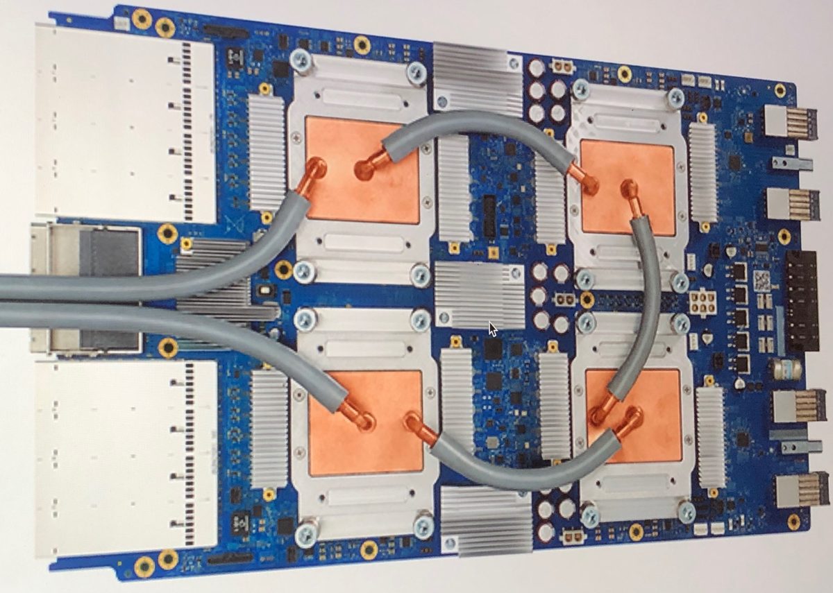
Image: Tensor Processing Unit 3.0(Zinskauf, CC BY-SA 4.0), Wikimedia Commons. A board photo of the datacenter-class TPU v3 — not the Edge TPU itself, but a reference showing the scale of the datacenter "parent" that shares the same systolic-array approach.

In 2019, Google launched the Dev Board and USB Accelerator carrying this Edge TPU (4 TOPS, 2W), and it drew a following as an add-on accelerator for existing SBCs like the Raspberry Pi, backed by power-efficient inference that could run MobileNet v2 at roughly 400 frames per second. Since then, though, Google has effectively stopped investing in the product line without shipping any notable new hardware, and as of 2026 its official coral.ai site redirects to a generic Google Developers page. The reason Coral products haven't fallen entirely out of use despite this is that Google released the drivers and firmware as open source, letting community projects such as the object-detection surveillance software Frigate NVR pick up support and keep the hardware alive in production (detailed further in the SBC comparison article).
Real-world example: nine neural networks running concurrently on a single Jetson TX2 aboard a Skydio X2 drone
A leading example of a single accelerator chip running multiple neural networks in parallel is the autonomous flying drone Skydio X2/X2D. The X2 carries an NVIDIA Tegra X2 — the same SoC found in the Jetson TX2 — as its main compute chip, processing feeds from six onboard cameras (three stereo pairs, a trinocular configuration) to run nine custom-designed deep neural networks concurrently, entirely onboard. Using these inference outputs, it can track up to 20 simultaneous objects of interest — obstacles, subjects such as people or vehicles — while building a 3D world model updated at a rate exceeding one million points per second, and the decision loop that turns that world model into flight commands runs at a rate of 500 Hz. The reason it can fly fast through dense forest or indoor spaces avoiding obstacles without relying on GPS is that this entire pipeline is completed on a single Tegra X2 onboard, rather than being offloaded to the cloud.
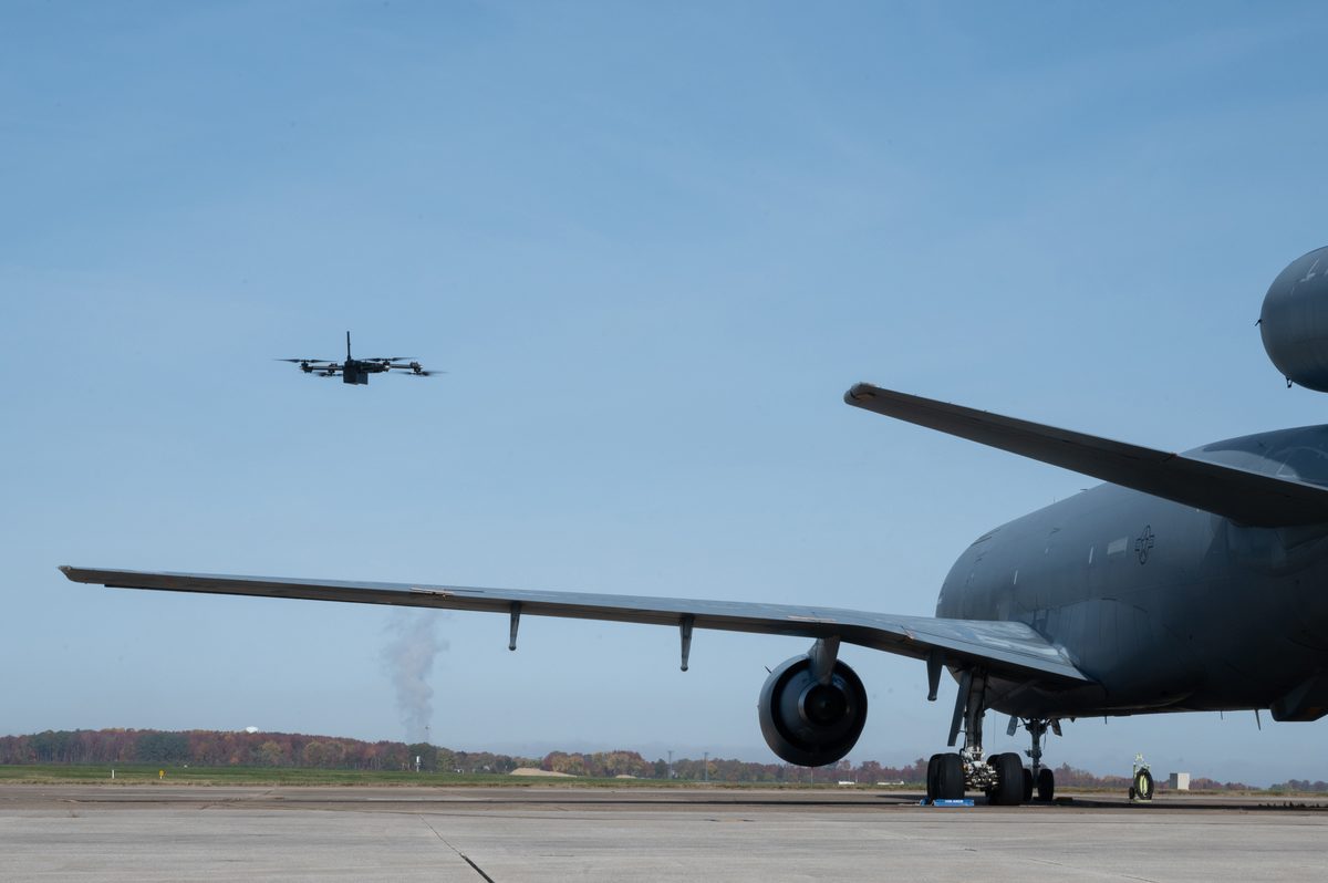 Skydio X2D inspecting a KC-10 Extender (Dover Air Force Base)
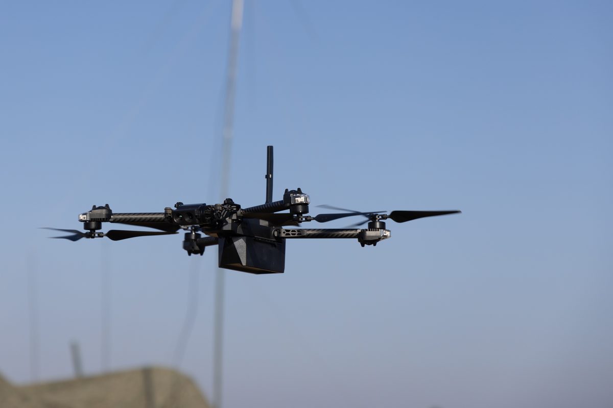 A Skydio X2D flying during training (Camp Schwab, Okinawa)
Images: Skydio X2D inspecting aircraft(Mauricio Campino, Public domain) / U S Marines Practice UAS Operations (9269101)(Public domain, U.S. Marine Corps), both via Wikimedia Commons.

.jpg)
The X2D designation refers to the Department of Defense variant, and real deployments recorded in publicly released U.S. DoD photos include the 436th Mission Generation Group at Dover Air Force Base, Delaware, using an X2D to inspect the structural integrity of a KC-10 Extender aerial refueling aircraft (November 2022), as well as the 5th Air-Naval Gunfire Liaison Company (5th ANGLICO) training at Camp Schwab, Okinawa, and the 10th Mountain Division training at Hohenfels Training Area in Germany, both operating the Skydio X2D as a small unmanned aircraft system (sUAS). Its successor, the X10, moves from the Tegra X2 to a Jetson Orin-generation SoC and upgrades its navigation cameras to 32 megapixels — a good illustration of how a jump in per-chip TOPS across generations translates directly into real operational gains: more neural networks running concurrently onboard, more simultaneously tracked objects, and a higher-frequency decision loop.
From a hobbyist's "AI appliance" to the frontier of on-device training
GPU-integrated accelerators once centered on robotics and defense applications have, by 2026, started reaching individual and small-scale developers as well. "ClawBox," built by Bulgaria's ID Robots, is an AI assistant hardware appliance carrying an NVIDIA Jetson Orin Nano, housed in a palm-sized enclosure with a cooling fan and side ventilation — reusing, as-is, the same SoM originally designed for robotics workloads. The fact that a chip designed to be the "brain" of a drone or industrial robot can be dropped directly into a product shipping in the hundreds or low thousands of units, made by a small startup, underscores the strength of GPU-integrated accelerators' generality — unlike a dedicated ASIC, they can run arbitrary CUDA models as-is.
A second, related trend is research pushing what was once a purely inference-only edge accelerator toward on-device training — retraining a model directly on the device. A paper published in July 2026, "Empowering On-Device Model Adaptation with an Edge AI Inference Accelerator" (Piechocki, Capotondi, Kraft, arXiv:2607.18101), proposes a pipeline using the Hailo-8L (a lower-tier sibling of the Hailo-8 discussed above) that splits inference and training work across chips: the quantized backbone's inference runs on the Hailo-8L, while only the lightweight final layers are fine-tuned incrementally in FP32 on the CPU. The paper reports up to a 15.4x wall-clock speedup for on-device training compared to a Raspberry Pi 5 alone — one glimpse of a research frontier where the very premise of "inference-only" is starting to erode, built on the same underlying technology stack of quantization and graph compilation.
Parameters that determine performance
- TOPS/W efficiency versus precision flexibility: The Coral Edge TPU is highly efficient at 2 TOPS/W, but that comes with the constraint of running only fixed graphs pre-quantized to INT8. The Jetson Orin NX, by contrast, can run arbitrary CUDA models in a mix of FP16/INT8, at the cost of falling short of Coral's TOPS/W. How much flexibility a project can afford to give up is usually the first fork in chip selection
- Compiler strictness: A fully fixed-graph compiler like the Coral Edge TPU Compiler, which allows no unsupported operators whatsoever, forces model design to be constrained to supported operators from the start. Partial-offload compilers like TensorRT/OpenVINO offer more porting flexibility, but it's easy to overlook the speed penalty that appears when a CPU fallback is triggered
- Choice of quantization method (PTQ vs. QAT): PTQ, needing only a small amount of representative data, is cheap to develop but prone to larger accuracy loss on models with many outliers. QAT costs a retraining pass but suppresses that degradation. VPUs of the Movidius Myriad X generation, built primarily around FP16, sidestep the calibration effort of quantization entirely by design
- Interface bandwidth: USB-connected devices like the Coral USB Accelerator or NCS2 can hit a host-side USB bus bandwidth bottleneck when several units are combined (detailed in the Frigate NVR case in the SBC comparison article). M.2/PCIe-connected devices like the Hailo-8, or SoM-integrated Jetsons, are less exposed to this constraint
- Supply continuity and roadmap: Intel's Movidius NCS2 is explicitly marked "Discontinued" on its own spec page, and Coral's official site now redirects elsewhere, while the Jetson line continues shipping new generations. For a long-running project, supply continuity itself becomes a risk factor beyond a one-off TOPS-per-dollar comparison
- Price-to-performance ($/TOPS): On a simple $/TOPS basis, the Jetson Orin Nano Super ($249/67 TOPS ≈ $3.7/TOPS) and Jetson Orin NX ($599/100 TOPS ≈ $6/TOPS) can look cheaper than the Hailo-8 ($110/26 TOPS ≈ $4.2/TOPS) or Coral ($75–99/4 TOPS ≈ $19–25/TOPS) — but the final choice still comes down to the balance against the chassis size and power budget a given product can actually accommodate, not raw performance and unit price alone
Does twice the TOPS mean twice the application speed?
Precision, memory, supported operators, transfers, and preprocessing affect speed. Measure end-to-end latency on the actual model.
References
- Neural Network Compression Framework (NNCF) — OpenVINO official
- OpenVINO (Wikipedia)
- Intel Neural Compute Stick 2 — Product Specifications (Intel official)
- Review: Intel Neural Compute Stick 2 for Edge AI (viso.ai)
- Intel to Acquire Computer Vision Company Movidius (Road to VR)
- Intel announces the Movidius Myriad X (Notebookcheck)
- Google Coral Edge TPU / Dev Board — CNX Software
- Coral Dev Board TPU (NXP)
- Cloud TPU system architecture (Google Cloud official)
- NVIDIA Jetson Orin NX 16GB Module Review (ThinkRobotics)
- NVIDIA Jetson Orin NX Series Data Sheet (NVIDIA Developer)
- Jetson Orin Nano Super Developer Kit (NVIDIA official)
- Inception Spotlight: Skydio 2 Drone Powered by NVIDIA Jetson (NVIDIA Technical Blog)
- Skydio X10 vs X2 comparison (THE FUTURE 3D)
- Empowering On-Device Model Adaptation with an Edge AI Inference Accelerator (arXiv:2607.18101)
- Sustainable LLM Inference for Edge AI (arXiv:2504.03360)
- Hardware PXL 20231201 152957218 (53388218926) — Wikimedia Commons
- Tensor Processing Unit 3.0 — Wikimedia Commons
- ClawBox AI assistant device (2026) - front — Wikimedia Commons
- Skydio X2D inspecting aircraft — Wikimedia Commons
- U S Marines Practice UAS Operations (9269101) — Wikimedia Commons
Current step · 21 / 21 · Sensors & Hardware
Comments
Please log in to post a comment
No comments yet.