Contents — find the section you need
Background and reading guide
Background No specialist background required; check the reporting period and scope of financial measures.
Industry research · Read the sources, reporting period and comparison criteria together.
Semiconductor manufacturing equipment builds microscopic circuits onto silicon wafers. Japanese companies have lost ground producing semiconductors themselves, but stay globally competitive in the equipment that makes them. Tokyo Electron, one of the largest full-line equipment makers in the world, and SCREEN Holdings, holding the world's top share concentrated in cleaning alone, diverge sharply in both scale and strategy. Tokyo Electron's coater/developer systems hold a 90% world share (nearly 100% for EUV lithography applications) — a degree of dominance that stands out even within the semiconductor industry — while SCREEN carries the unusual history of a printing company that transformed itself into a semiconductor equipment maker.
 Tokyo Electron
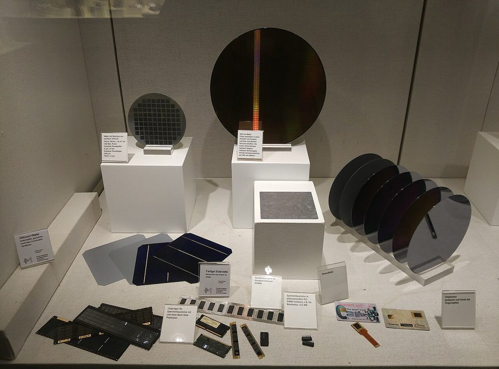 SCREEN Holdings
Image: Tokyo Electron logo (public domain; trademark rights still apply separately) / Silicon wafers (CC0), Wikimedia Commons. The wafer photo is not a specific SCREEN product — it illustrates the kind of object SCREEN's cleaning process works on.


Company History: Tokyo Electron's Semiconductor-First Founding, SCREEN's Pivot From Printing
Tokyo Electron was founded on November 11, 1963, in Akasaka, Minato Ward, Tokyo, with ¥5 million in capital, by Tokuo Kubo, Toshio Kodaka, and others under the conviction that "semiconductors will transform industry" — initially as a specialized technology trading company. It began business in 1964 by securing import and distribution rights for diffusion furnaces from Thermco of the U.S., then moved into domestic manufacturing of diffusion furnaces through a joint venture, Tel-Thermco, in 1968 — the start of its transformation into an equipment maker. In 1986 it took full ownership of a joint venture with Lam Research of the U.S. to expand its own product lineup, began exporting overseas that same year, and reached the top spot in the world by semiconductor equipment maker revenue in 1989. In 2013 it signed a merger agreement with Applied Materials of the U.S., but the deal was called off in 2015 over antitrust concerns; since then, the company has pursued growth independently under successive visions and mid-term management plans.
SCREEN Holdings traces back further, to 1868 (the first year of the Meiji era), when copperplate engraver Saijiro Ishida founded a lithographic print shop, Ishida Kyokuzan Printing, in Kyoto. After passing through the copperplate- and lithographic-printing eras, the company succeeded in domesticating "photoengraving glass screens" — essential for photographic printing plates — and in 1937 spun off its research division as Dai Nippon Screen Manufacturing, incorporating as a stock company in 1943. The company's name, "Screen," comes from this founding business, the glass screen. It later diversified into precision components — electronic engraving machines, target meshes for TV camera tubes, shadow masks for color CRT televisions — and in the 1970s entered the semiconductor equipment business, developing photoresist coating systems and batch-type cleaning systems. By 1994, revenue from electronics equipment had overtaken its founding printing-equipment business, completing a total shift in its core business. On October 1, 2014, the company renamed itself SCREEN Holdings Co., Ltd. and transitioned to a holding-company structure.
Comparing Company Scale: Five-Year Trend
Both companies' fiscal years end in March. Tracking the last five fiscal years (FY2022/3 through FY2026/3) shows both companies riding the same semiconductor investment cycle, with the gap in scale between them staying roughly constant throughout.
| Fiscal Year | Tokyo Electron Revenue | Tokyo Electron Operating Profit | SCREEN Revenue | SCREEN Operating Profit |
|---|---|---|---|---|
| FY2022/3 | ¥2.0038 trillion | ¥599.3 billion | ¥411.9 billion | ¥61.3 billion |
| FY2023/3 | ¥2.2090 trillion | ¥617.7 billion | ¥460.8 billion | ¥76.5 billion |
| FY2024/3 | ¥1.8305 trillion (a down cycle) | ¥456.3 billion (down) | ¥504.9 billion | ¥94.2 billion |
| FY2025/3 | ¥2.4315 trillion | ¥697.3 billion (peak) | ¥625.3 billion (peak) | ¥135.7 billion (peak) |
| FY2026/3 | ¥2.4435 trillion (slight increase) | ¥624.9 billion (down) | ¥605.7 billion (down) | ¥122.5 billion (down) |
| Metric | Tokyo Electron | SCREEN Holdings |
|---|---|---|
| Net profit (FY2026/3) | ¥574.4 billion (+5.6% YoY, partly on gains from selling cross-held shares) | ¥92.0 billion (-7.5% YoY) |
| Consolidated employees | 19,573 (as of FY ending Mar 2025) | 6,884 (+469 YoY) |
Tokyo Electron's revenue runs roughly 4x SCREEN Holdings'. What's striking is that both companies followed almost the identical cycle — a slump during the FY2024/3 semiconductor investment downturn, a sharp rebound to record territory in FY2025/3, and a swing back to declining profit in FY2026/3. The gap in headcount (about 2.8x) is smaller than the gap in revenue (about 4x), putting SCREEN somewhat lower on revenue per employee. Tokyo Electron still grew net profit in FY2026/3, helped by gains from selling cross-held shares, while SCREEN saw both operating and net profit decline.
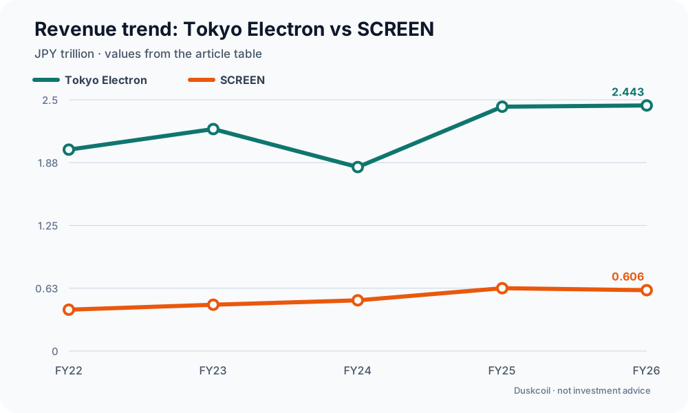
Diagram: Duskcoil. Revenue values in the article table, converted to JPY trillions. This diagram is not investment advice.
Comparing Flagship Products
Coaters/Developers vs. Cleaning Equipment: Each Company's Own Near-Monopoly
Among Tokyo Electron's product lines, the standout is the "coater/developer" system, which applies photoresist to the wafer and develops it after exposure — its flagship product family, "CLEAN TRACK" (including the LITHIUS Pro and ACT series). Its world share sits at roughly 90%, rising to nearly 100% for the most advanced EUV lithography processes, built on tight integration with ASML of the Netherlands, the world's leading lithography-equipment maker; the ability to link directly in-line with the exposure tool and optimize the whole process is Tokyo Electron's core competitive edge here.
SCREEN Holdings' cleaning equipment holds the world's top share (34.7%) across all three categories: single-wafer systems (flagship products SU-3200, SU-3300, and SU-3400), which process one wafer at a time; batch systems, which process multiple wafers at once; and spin scrubbers, which clean substrates while spinning them at high speed. Cumulative shipments passed 15,000 units in 2025, and the company is especially competitive in single-wafer cleaning equipment for leading-edge logic and memory chips. The SU-3300 uses SCREEN's proprietary "Advanced Process Atmosphere Control" technology to keep the interior of the chamber at an ultra-high-purity state, achieving throughput that approaches batch systems while retaining the higher cleaning quality unique to single-wafer processing.
| Item | Tokyo Electron Coater/Developer (CLEAN TRACK) | SCREEN Single-Wafer Cleaning Equipment (SU-3300 and others) |
|---|---|---|
| World share | ~90% (nearly 100% for EUV applications) | 34.7% across all cleaning equipment (world's top share across single-wafer, batch, and spin-scrubber categories) |
| Primary use | Resist coating and development, in-line integration with lithography tools | Removing impurities and residual chemicals from wafers, for leading-edge logic/memory |
| Source of competitiveness | Whole-process optimization through integration with ASML's lithography tools | Proprietary chamber-atmosphere control technology combining high throughput with high quality |
Etching and Deposition vs. a Push into Back-End (Advanced Packaging)
Tokyo Electron is a full-line equipment maker with products across all four major front-end process steps. Beyond the coater/developer, its lineup includes the "Tactras" plasma etching system (launched in 2006, a 300mm-wafer-capable machine that can house up to six etch chambers) and the "Triase+" single-wafer CVD deposition system, which uses WF6 and TiCl4. In both the etching and deposition markets, Tokyo Electron holds an oligopolistic position alongside Applied Materials and Lam Research of the U.S.
SCREEN has traditionally concentrated its business on the front-end cleaning process, but in recent years it has been expanding into back-end processes — particularly advanced packaging, the technology that stacks and connects semiconductor chips. At SEMICON Japan in December 2025, the company laid out two new directions built on its track record of more than 15,000 cleaning-equipment units shipped: a push into back-end processes, and a new R&D facility in the United States. SCREEN's move beyond its front-end specialty into back-end technology reflects an industry shift in which, as AI chips grow more sophisticated, packaging technology itself increasingly determines performance.
A Difference in Technology Strategy
Making a semiconductor takes dozens to hundreds of process steps — deposition, photolithography (coating and development), etching, cleaning, thermal processing, and more. The two companies' strategies diverge sharply on how much of that process each one covers.
Tokyo Electron is a full-line equipment maker with products across all four of the major semiconductor process steps — deposition, coating/development, etching, and cleaning — holding a world-leading share in many of them. A product portfolio that isn't tied to any single process step gives it the strength to spread out its exposure to a shift in any one technology trend.
SCREEN Holdings, in contrast, started out as a specialist focused on a single process — "cleaning," which washes impurities and residual chemicals off the wafer. By narrowing its focus to one process, it sharpened its technology deeply, turning the ability to customize for each customer's specific needs into its core competitive edge. As noted above, though, its recent push into back-end processes is gradually broadening that once-narrow specialty.
This contrast — broad-and-shallow versus narrow-and-deep — is a pattern seen across the semiconductor equipment industry as a whole, and the two companies are often positioned less as direct rivals than as players with different strengths at different points in the process.
Development & Manufacturing Facilities
Beyond its Tokyo headquarters in Akasaka, Minato Ward, Tokyo Electron operates production facilities through group companies in Yamanashi Prefecture (Tokyo Electron Technology Solutions, deposition and etching systems), Miyagi Prefecture (Tokyo Electron Miyagi, plasma etching systems), and Iwate Prefecture (Tokyo Electron Tohoku). Beyond its Kyoto headquarters, SCREEN Holdings operates its Hikone site (Shiga Prefecture) — the mother factory for its semiconductor manufacturing equipment — plus its Yasu site (Shiga Prefecture) and Rakusai site (Fushimi Ward, Kyoto) domestically. The map below plots the major domestic facilities we could confirm (overseas facilities and small sales-only offices are out of scope).
Sources: for Tokyo Electron, the official "Locations" and facilities pages plus the official pages of each group company (Tokyo Electron Miyagi, Tokyo Electron Technology Solutions). For SCREEN Holdings, the official "Domestic Facilities List" page. Some facilities at both companies do not disclose a precise street/lot number; in those cases the town/block-level location was confirmed via map/directory services (Mapion, NAVITIME, etc.). Coordinates were geocoded to town/block level via OpenStreetMap Nominatim.
Strategy & Outlook
Tokyo Electron's mid-term management plan, announced in June 2022, targets ¥3 trillion in revenue and an operating margin of 35% or higher for FY2027/3. Over the plan period it aims to invest more than ¥1 trillion in R&D, including more than ¥400 billion in capital expenditure, strengthening production capacity and R&D capability at the same time. In its July–September 2025 quarterly results, the company reaffirmed confidence in reaching the ¥3 trillion target, driven by expanding generative-AI demand, and frames semiconductor miniaturization plus growing AI-related demand not as a passing boom but as a structural shift likely to persist for a decade or more.
SCREEN Holdings, under its mid-term management plan "Value Up Further 2026," has set a longer-horizon target of ¥1 trillion or more in revenue and an operating margin of 20% or higher by FY2033/3. Over the three years from FY2025/3 through FY2027/3, it plans to allocate roughly ¥360 billion — combining operating cash flow and cash on hand — across capital expenditure (~¥100 billion), R&D (~¥110 billion), strategic investment (~¥80 billion), and dividends (~¥70 billion). Beyond the push into back-end processes noted above, the company has also announced plans for a new R&D facility in the United States, aimed at starting development earlier on core technologies — cleaning, thermal processing, advanced packaging — and shortening equipment-development cycles; the strategy is to gradually widen its business scope while preserving the strengths of a focused specialist.
The tailwind both companies share is the rapid expansion of demand for generative-AI-related semiconductors. AI chips demand advanced manufacturing on two fronts at once — finer circuit geometries and more sophisticated packaging — so Tokyo Electron's front-end equipment and SCREEN's cleaning and back-end equipment both play roles essential to improving AI-chip performance. At the same time, both companies experienced declining profit during the investment-cycle downturns of FY2024/3 and FY2026/3 — a reminder that as equipment makers, neither can escape the structural fact that their results are tightly coupled to the capital-spending cycles of the chipmakers they sell to.
References
- Tokyo Electron Official Site / Investor Relations
- SCREEN Holdings Official Site / Investor Relations (Japanese)
- About Tokyo Electron (Business Overview, Japanese)
- SCREEN Holds the World's Top Share in Semiconductor Cleaning Equipment (Japanese)
- Tokyo Electron History (official site, Japanese)
- SCREEN History (official site, Japanese)
- IRBANK: Tokyo Electron (8035) financial results (Japanese) / IRBANK: SCREEN Holdings (7735) financial results (Japanese)
- Tokyo Electron Coater/Developer CLEAN TRACK LITHIUS Series (Japanese)
- Tokyo Electron Etching Tactras Series (Japanese)
- Tokyo Electron Deposition Triase+ Series (Japanese)
- SCREEN Single-Wafer Cleaning Equipment SU-3300 (Japanese)
- SCREEN Group: From 15,000+ Cleaning Equipment Units to Back-End Processes and U.S. R&D (SEMICON Japan 2025 report, Japanese)
- Tokyo Electron Facility Locations (careers site, Japanese)
- SCREEN Holdings Domestic Facility List (Japanese)
- Tokyo Electron New Mid-Term Management Plan (FY2027/3 targets, Japanese)
- SCREEN Holdings Mid-Term Management Plan "Value Up Further 2026" (Japanese)
Current step · 5 / 21 · Corporate Research
Comments
Please log in to post a comment
No comments yet.